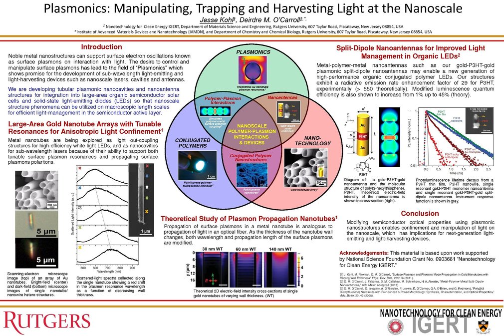
Plasmonics: Manipulating, Trapping and Harvesting Light at the Nanoscale
Light is the fastest means of sending information. However, there is a fundamental mismatch between the current ability to miniaturize electronic circuitry and the ability to confine light. Optical devices such as light lasers and optical fibers cannot have dimensions smaller than half the wavelength of light (sub-micron), whereas electronic circuitry can be made much smaller (nanoscale). Plasmonics is the science whereby conventional light (photons) can be ‘squeezed’ into nanoscopic volumes, much smaller than the wavelength. This is achieved by coupling photons to free electron oscillations of a metal, which propagate along the metal-dielectric interface. This phenomenon will allow electromagnetic signals traveling at the speed of light to be confined on length-scales unachievable with conventional optics and usher in the age of integrated opto-electronic circuitry and ultra-fast computing. Additionally, the ability to manipulate light on the nanoscale will improve the light the harvesting capability of solar cells, and the efficiency of solid state light-emitting device (LED) lighting and lasers. The primary focus of this research is on nanoscale engineering of light generating and light harvesting processes in organic polymer semiconductor materials and plasmonic nanostructures. We study the fundamental photophysics of polymer semiconductors and plasmonic nanostructures for the development of nanoscopic light-emitting devices such as nano-lasers, nanoscale antennas, waveguides and cavities. These nanoscopic devices are integrated into large area opto-electronic devices such as solar cells and LED’s so that nanoscale structure phenomena can be utilized on macroscopic length scales to improve opto-electronic device efficiency and enable efficient light-management in the active semiconductor devices.


Judges and Presenters may log in to read queries and replies.