
Nice work with potential promise for applications.
Since the use of solar cells is largely determined by cost vs. performance, can the nanostructure features be added in a cost effective way?
Judges’ Queries and Presenter’s Replies
Presentation Discussion
-

-

Thanks you for the question!
This is the most important question of all my research, and I believe the answer is an emphatic “Yes”
First — the design was chosen because it allows thinner, lower quality materials to be used. This reduces the baseline material cost
Second — fabricating the nanorods relies first on a liquid based process with silica nanoparticles in solution(which are readily available and inexpensive) that act as an etching mask, followed by reactive ion etching, which is an established technique used in fabrication of memory chips and micro-electromechanical-systems, followed by a wet etching step which is common to all electronics.
Cutting to the chase — our proposed fabrication method does not add significant challenge to current thin film fabrication procedures, but does have significant potential to improve efficiency, all the while using less expensive materials, so we believe it will be a very cost-effective option.
-

Terrific presentation and exciting work.
Would you be able to explain a bit what kind of simulation you have used?
Thanks! -
Thank you for the kind words.
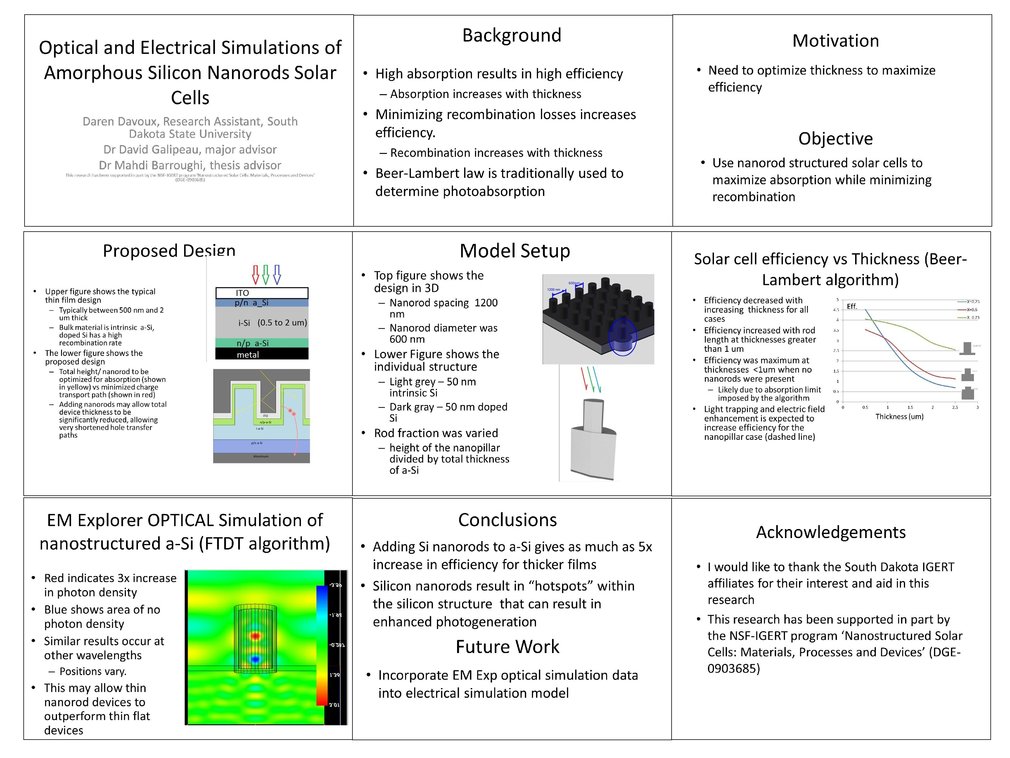
Our simulation examines the solar cell from two directions, optical and electrical.
Optical simulation involves determining how light will reflect off the surface and propogate through the material. Because the device has repeating, nanometer scaled structures on the surface of the device, determining the propogation of light through the device requires evaluation from a quantum mechanical perspective. EM Explorer is our software of choice. It parses the structure into hundreds of “Yee Cells” — cubicle partitions that make up the whole. Imagine how Lego blocks are used to form statues at Legoland. Once the device is parsed into these Yee cells, the electromagnetic equations (Maxwell’s equations) at each interface are solved systematically. After these are solved for each Yee cell, the Poynting vector in each Yee cell is known, which can be used to determine the photon density throughout the structure.
The Electrical simulation does similar. It divides the structure into small partitions, and systematically solves the propogation of charges and the resulting electric field throughout the structure (this leads to a voltage/current graph which can be used to find photovoltaic efficiency). Silvaco ATLAS is our software of choice.
The optical and electrical simulations merge. in areas of high photon density (as determined by optical simulation) there is a high photogeneration rate, which corresponds to a lot of excited electrons and free holes. These are then parameters for the electrical simulation, which answers the question “ok, I have a lot of electrons in this area of the structure, where do they go? where do they travel? and how do they influence the voltage at the terminals of the device?”
I hope I have answered your question. If not, I can probably offer you some caffeine to wake you up from the Grecian diatribe.
-
Further posting is closed as the event has ended.
Judges and Presenters may log in to read queries and replies.